
By Roger Griesemer, General Manager Memory Solutions, Swissbit AG and
Ulrich Brandt, Technical Director Marketing, Swissbit AG
3D NAND is a popular topic on websites, in magazines, in advertisements and at conferences. In the discussion surrounding 3D NAND, there is one common theme: it has a promising future. Within a few years, the technology has evolved from the original 32 layers, increasing first to 48, then to 64. 3D NAND currently has 96 layers. This will continue to grow, with the next generation, only a few months away from release, set to contain 128 layers.
Vertical stacking was the perfect solution to the increase in miniaturization of components, heightened risks and rising costs. Sub 10nm NAND was deemed unachievable, both commercially and technologically.
The market saw a significant drop in the cost of SSDs and storage cards. This was caused by a combination of reduced manufacturing of stacks in excess of 64 layers and an oversupply driven by higher chip capacities. The 3D cell had a larger capacity, thanks to a superior physical build over the 2D cell. This made way for the introduction of QLC products; 4 bits per cell with 16 voltage levels that need to be distinguished reliably. Designs with 5 bits per cell (PLC = Penta Level Cell) are already being developed.

64 cell comparison between 2D & 3D NAND
It’s safe to say that 3D NAND has conquered the storage world and is very well positioned. This is particularly the case for consumer or enterprise SSDs that typically sit within well-ventilated systems.
However, what happens if you use a consumer 3D NAND SSD for typical industrial applications? Those that are within tight vent-less systems and often used outdoors and subjected to frequent and extreme temperature variations? Those applications need to log data from a multitude of sensors with a high data rate of small transfers? How does 3D NAND meet these requirements?
Let us start with a few common statements about 3D NAND:
- 3D NAND is more reliable than 2D NAND
- 3D NAND is faster than 2D NAND
- 3D NAND is cheaper than 2D NAND
The last statement is unquestionably accurate given the current 3D NAND designs. After all, that’s exactly what NAND manufacturers wanted to achieve with their billions of dollars of investments into the technology. The other two statements require a little more insight.
Is 3D NAND more reliable than 2D NAND?
It is often suggested that 3D NAND is more reliable than 2D NAND because the active area of the cell and the size of the storage plate is significantly greater in 3D NAND. The cell in 2D NAND is comprised of a small flat area; whereas the cell in 3D NAND wraps around the bit line, allowing for more charge to accumulate. In 3D NAND, electrical interference from adjacent cells could be reduced and the signal to noise voltage ratio improved; this all sounds promising. This advantage, however, was used to achieve greater bits per cell and cost reductions and not necessarily increased reliability.
2D NAND MLC technology typically has an endurance of 3000 programs/erase cycles, meaning each block can be erased and reprogrammed 3000 times before the cell degrades so far that its storage capacity of one year can no longer be guaranteed.
3D NAND should achieve a higher number of program/erase cycles. However, typically, only 3D TLC NAND versions are offered. Cell capacity improvements have been used to increase bits-per-cell, and as a result, 3D NAND also offers 3000 programs/erase cycles identical to 2D NAND. This was only achieved incidentally through various modifications, particularly regarding error correction.
Whilst the 2D NAND’s 3000 program/erase cycles are reached with a simple 40-bit per 1KiB BCH error correction, 3D NAND requires at least a 120-bit error correction to be able to match the 3000 cycles. This is a new process called LDPC, that requires a lot more check bits, and therefore more silicon area in the controller and more computing time of the correction firmware. This is especially the case when the number of faulty bits increases towards the end of life. Older controllers do not have the required resources and therefore won’t work with 3D NAND.
With the new 3D NAND technology, new error mechanisms have appeared in the Flash. Consequently, new firmware functions such as Block RAID, are now required. This feature prevents the failure of an entire block which previously was neither possible nor necessary.
Without this feature, system failures can occur in the range of up to 1000 DPPM (1000 failures per million devices). This is acceptable for consumer products and block RAID is usually not implemented. However, such an error rate is not acceptable for industrial products.
Here, the correction of block failures is mandatory and requires great efforts both in the firmware and in the provision of greater redundancy. The feature protects customers from unexpected failures in the field. With error rates at 1000 DPPM level, potential risks cannot be discovered during normal qualifications. Customers must rely on the SSD manufacturer to have taken all necessary measures to minimize field failures.
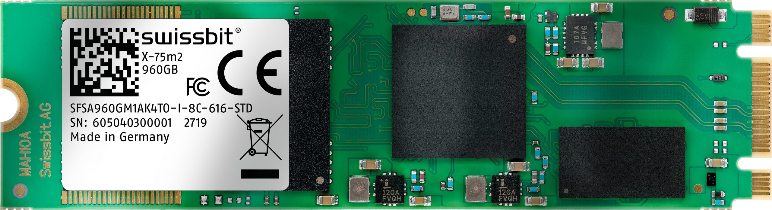
Swissbit X-75m2 Industrial M.2 SATA Solid State Drive (SSD) module available in storage capacities from 30GB to 960GB that deploys 3D NAND technology and AES256 encryption.
The advantage of block repair, however, also comes at a price: additional memory is required to save parity information. This increases the Write Amplification Factor (WAF), which in turn reduces the lifespan of the SSD. The larger the WAF, the lower the life expectancy. For this reason, many consumer products avoid this feature. Industrial SSDs on the other hand, need block RAID or an equivalent error handling, making them more complex and resulting in a significantly higher qualification effort.
Cross-temperature
A further aspect of 3D technology is its behavior during temperature changes, otherwise referred to by its technical term, cross-temperature.
With 2D NAND, the conformity of all cells was defined by the optical lithography’s accuracy. A reasonable assumption is that the cell properties of all cells in an array were identical. Whilst the cells did not have a high capacity, they were at least equal within a page.
Whilst 3D NAND has much better cell properties, it’s also characterized by much higher variations.
Let’s picture a 3D NAND bitline as a tiny hole that is etched through 64 layers. Ideally, the hole would be the same size at the top layer as it is at the bottom of the stack. However, the reality is very different: the top layer has a much larger diameter than the bottom, resulting in completely different cell capacities and voltage thresholds. All 64 cells between the top and bottom layers belong to the same bitline and the same voltage detector. As a result, voltage levels within this bitline vary greatly and must be permanently compensated. Now add in temperature variations, and the work of the detector becomes very difficult. For example, when writing at low temperatures and reading at high temperatures, the voltage ratio is completely different than when the order is reversed.
Generally speaking, all extreme temperatures are critical for 3D NAND. Operation below -10°C or at 85°C will cause read problems by shifting the voltage level. If there is further interference due to intensive reading or a power failure, data loss is inevitable.
For the standard consumer, 3D NAND flash, the permitted fluctuation between the write and read temperature is about 45 to 50 Kelvin (K). This means, for example, you can write at 20°C and read at 65°C, which is sufficient for consumer products.
In contrast, industrial applications with a specified ambient temperature operating range between -40°C to 50°C easily reach an SSD temperature range between -40°C and 85°C. This is 125K cross-temperature and 2.5 times the range of a consumer drive, which will most likely fail under these conditions.
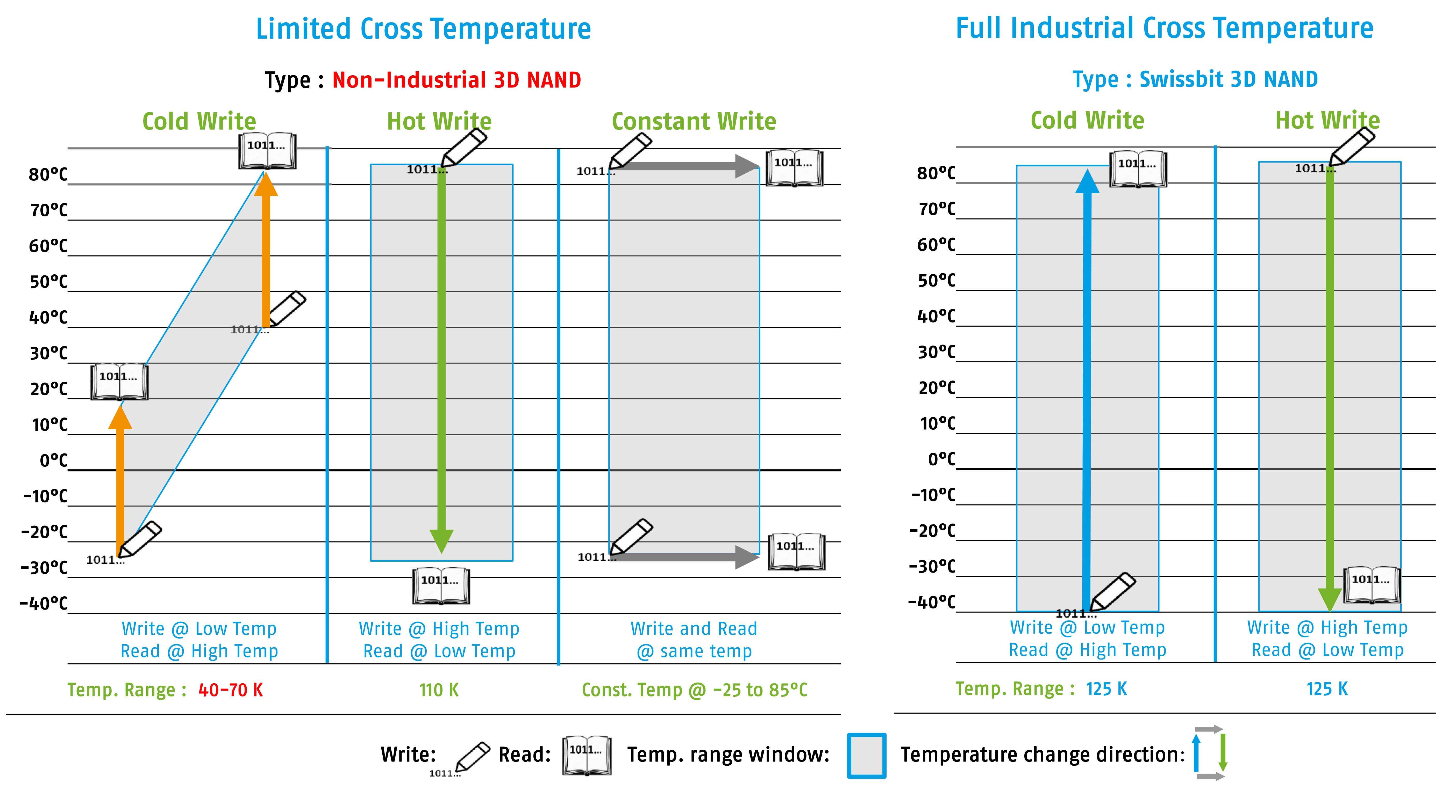
Cross temperature behavior
Very few specially tuned 3D NAND products that meet these specifications are available on the market. They are more expensive but offer safety against data loss.
3D NAND offers higher reliability on an individual cell level than 2D NAND, but the high stack-up and transition to TLC negate any performance improvements, thereby requiring additional mechanisms to match the reliability of 2D NAND. Only by implementing the correct NAND can industrial-grade products be manufactured.
Speed characteristics
It is true that 3D NAND technology offers a faster Write speed than 2D NAND. This is because all three bits of the 3D cell can be written in a single process step. In contrast, 2D NAND requires two programming steps to write each bit – first the lower (fast) bit followed by the upper bit in a separate programming step.
Whilst each individual step is faster in 2D NAND, 3D NAND is faster in the total time that it takes to write 3 pages (3 bits).
What if there aren’t three pages readily available for writing? This can often be the case with random writes of small data packages. In this case, the addition of dummy pages is needed to fill the 3 bits. Writing with dummy pages reduces the effective data rate compared to 2D NAND.
DRAM cache is often used as a countermeasure to be able to collect pages over a longer period of time in order to write three information pages at a time. This makes the SSD more expensive. In addition, the controller needs enough buffer space for three pages, which older controllers don’t offer.
A common solution is to use a small portion of the memory as an SLC cache. The write performance is very high at the beginning. As soon as the cache is full, 3 pages from the pSLC area are converted into a TLC page. Once this process begins, the drive slows down significantly. Each new data transfer causes pSLC pages to be converted into TLC. Another option is to use the complete memory in pSLC mode, to begin with. The cache in this instance is much larger than in the previous case. 1/3 of the drive capacity is available as fast storage. Additional capacity requirements kickstart the conversion process from pSLC to TLC.
Benchmark tests are often based on small storage capacities and are usually carried out with “Fresh out of the box (FOB) = as yet unused” SSDs. Here, the complete SLC cache is still available and impressive measurements can be taken. Over the lifetime, the performance drops down to a fraction of the specified values.
A third solution is called ‘TLC direct’. Here, the SLC cache is not used and programming is performed as a one-step process. As previously mentioned, a DRAM is needed for the process to work efficiently. Even then, the top speed is reduced compared to the SLC caching option. However, the performance remains largely constant over the entire service life.
As can be seen from the above descriptions, speed is not necessarily constant when using a memory drive. Impressive specifications do not mean that they are maintained as the drive is filled.
For industrial applications, performance consistency is more important than maximum performance. For this, the firmware needs to be optimized according to the application requirements. Drives for industrial applications are finetuned for constant data rates and long service life.
Endurance
The endurance of 2D NAND drives was measured relatively easily by letting the required test run for an extended period of time. Then, with the use of tools, the number of internally and externally written pages was determined (the term for this ratio is WAF) and finally the expected possible Terabytes written (TBW) extrapolated.
With 3D NAND, many new aspects influence the endurance of the drive. Essentially, the more flash that is written internally as a result of an external data transfer, the lower the expected TBW.
Endurance is reduced by:
- Block RAID, as additional pages are needed for parity
- SLC Cache, because each logical page will be written at least twice in the flash
- DRAM-less drives, often requiring dummy page writes.
Endurance is often also influenced by:
- The memory size effectively used by the benchmark
- Preconditioning of the drive (FOB vs already written)
- The benchmark profile (small vs large block size, use of TRIM, flush cache).
In summary, the endurance of SSDs with 3D NAND flash is comparatively lower than a drive with 2D MLC, even though both NAND components are specified with 3000 erase cycles. Consumers are more interested in cost per GB than the cost per TBW. For industrial drives that operate for many years in the field, the cost per TBW is much more important than the initial purchase price of the drive.
Error correction
As already mentioned, 3D NAND needs a much higher number of bits for error correction.
120-bit LDPC is needed instead of 40-bit BCH.
Initially, this may not appear to be so important. However, the consequences are a lot more complex. Going from 40-bit BCH to 120-bit BCH would require not just a 3-fold, but more than a 10-fold bigger chip surface area. This is not only very expensive but also difficult to achieve.
The solution is a new code procedure, initially used in 2D TLC: LDPC (low-density parity-check). Only a few bits are used for the checksum generation, but this requires so-called soft information from the NAND. Instead of getting all the correction information with a simple read, three read accesses are now needed to repair a maximum of 120 faulty bits. While a small number of bit errors can be corrected by the LDPC hardware, the controller needs software algorithms when the number of errors is higher. As a consequence, the memory slows significantly when the bit error rate increases, due to aging. In fact, significantly slower than with 2D NAND.
New controllers – new features
One improvement that has resulted from the additional requirements demanded from modern 3D NAND controllers is End-to-End data path protection or E2E DP. In older controllers, the internal RAM for the page buffers, the data path between the different units, and the DRAM content were not protected against bit fails (for example as a result of radiation or alpha particles).
Undetected data corruption poses a high risk because it can lead to incorrect settings or wrong results. An undetected single bit fails could cause significant financial or even physical damage were it to happen with bank transactions, medical treatments, or robot control.
The latest controllers protect all data paths with parities. All buffer areas and DRAM content are secured by ECC (Error Correction Code).
Errors no longer go undetected, and in most cases rejecting and repeating a write command or marking the read data as defective can prevent further processing of the incorrect data.
Conclusion
For industrial SSD’s, the firmware and NAND architecture need to be fine-tuned to achieve high endurance, consistent performance, and stable operation within the industrial temperature range.
The sacrifices to be made are a limitation in top performance and higher purchase prices. The advantages, however, are robust products with low life cycle costs due to greater endurance and reliability.
Swissbit has more than 20 years’ experience in designing products for industrial applications and offers a variety of drives that are optimized for endurance, life cycle costs, and robustness.
About the Authors
 Roger Griesemer
Roger Griesemer is a proven electronics industry expert who joined Swissbit AG in 2003 and helped to shape the company during its startup years. He was appointed General Manager of the Memory Solutions division in July 2019. Roger’s contributions as Head of Product Management and Business Unit Manager were instrumental in establishing the company as the only European provider of real industrial products and solutions for data storage.
Roger can be reached online at [email protected] and at the company website http://www.swissbit.com/
Ulrich Brandt
 Ulrich Brandt is Director Technical Marketing at Swissbit AG. With more than thirty years of experience in-memory architecture, DRAM chip design, application engineering, and technical marketing, he was until recently responsible for the DRAM business unit at Swissbit. He holds a master’s degree (Dipl.Ing.) in electrical engineering from the Technical University in Braunschweig, Germany.
Ulrich can be reached online at [email protected] and at the company website http://www.swissbit.com/
64 cell comparison between 2D & 3D NAND
Cross temperature behavior.
Swissbit X-75m2 module
